Okay, so when we last left off, I had discovered an unfortunate mistake in the original PCBs I had recreated for my TV Typewriter project: they were too small, a victim of the distortions that happen when ‘line art’ is scanned.
It’s all good. As I mentioned also, I had managed to run into some actual vintage 1973 board stock. Now re-doing my work was no longer a matter of desire – it was necessity, just to get that inch or so closer to a full replica.
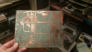
If you read my post about my 2-5-2-2 toner transfer process you’ll see the first board I worked on – a redo of the TVT mainframe board. But the TVT gremlins weren’t going to let me off that easy — it turned out, after etching, that it was still the wrong size! Apparently printing onto magazine paper causes some kind of weird dimensional loss. I suspect it may be because the inks used to print on magazine paper are water based and perhaps the heat from the laser printer causes a bit of that to boil off and thus shrink? Not sure. Anyway, after some trial and error I figured out the loss was about 1% all around. Adjusting for this and reprinting gave me the right dimensions, and finally the correct size board.
Now, I mentioned before that these vintage copper clad sheets, which I was lucky to find, were only 0.03″ thick. That’s a problem, because most PCBs commonly are around 0.06″ thick. And we want that thickness, because the TVT has some heavy components, like the transformer, and we don’t want any flex. So what I decided to do was etch my PCB pattern on one board, and then completely etch off the copper on another, and then cut to size and sandwich them together with epoxy. This seemed straightforward enough, and so I trundled ahead — made my first mainframe board and then epoxied together. And it looked good until I noticed that bubbles were forming internally. And no matter what I did, I couldn’t make them go away. The result was a splotch effect that made the board look obviously glued together.
Nope. Don’t want that. It was suggested to me that I buy a book press. Apparently you want to apply a huge amount of pressure to prevent bubbles from forming. I couldn’t find one though – not one that wouldn’t incur a fortune in shipping fees from the U.S., which was the only place I could find them.
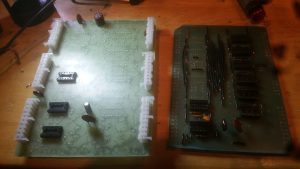
So I played around. On the mainframe board, I actually ripped it apart (the epoxy is suprisingly easy to remove once exposed), cleaned and retried, this time waiting a little while before bonding the two boards. This helped, but there’s still some discoloration. I must have tried four different ways on five different boards before realizing there wasn’t much I could do. My final trick was to switch to contact cement. This made a world of difference – on my cursor board, it left it looking mostly like an original piece of 0.06″, save for a couple of splotches or ‘birthmarks’, as I like to call them. I decided to accept that and move on. A couple of boards I did – my Memory and Timing boards, I actually started drilling right after bonding, and this produced a kind of ‘craquelure’. Here’s a picture of the ‘new’ timing board, next to the old one as I’m stripping the part. Notice the ‘cracks’.
Oh well — over time they faded and now, frankly, I don’t notice them. On my final board, the Cursor, I waited a full 15 minutes after applying the cement to both boards and then attached them. This made for a much cleaner look, albeit with some ‘birthmarks’. I decided to live with those. This TVT will live inside a case anyway. I doubt anyone but the most discerning will bother to note the splotches. Alright, now to actually follow the directions this time and start building. Here comes the mainframe!


